STM32 Development with CubeMX and Eclipse
First Steps
Now you can begin with a simple program for the STM32. This is done by first calling CubeMX once and selecting the option New Project on the home page. Next select the controller to be used. In order to make the selection easier, filter the list in the upper most line according to the relevant model lines or search for the necessary peripherals using the settings in the left hand column.
For the STM32F103C8T6 module, select the STM32F1 series in the topmost line under Series and refine the selection to the STM32F103 Line. Afterwards the desired selection STM32F103C8Tx appears at the far right.
The manual (STM document UM0919) explains that the STM32VLDiscovery involves an STM32F100RBT6B (STM32F1 series, STM32F100 value line). You'll also learn that the module has two LEDs PC8 (blue) and PC9 (green) as well as a button that is connected to PA0.
After you've selected the model, CubeMX downloads libraries as needed from the Internet. The program then shows something like what you can see in Figure 2. You will find yourself in the Pinout tab. Here you will see the chip and its connections to the right. To the left, the program itemizes the resources for the controller in a list arranged according to functionalities.
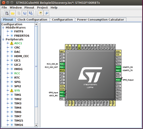 Figure 2: CubeMX with the Discovery Board pin allocation.
Set up the corresponding configuration files (Listings 4 and 5) for the STM modules STM32F103C8T6 or STM32F030F4P6. Copy these to the board folder already created by the system. If you do not have the necessary administrative rights, you will need to specify the complete path to the relevant file when calling OpenOCD.
Listing 4
STM32F103C8T6.cfg
source [find interface/stlink-v2.cfg]
transport select hla_swd
set WORKAREASIZE 0x2000
source [find target/stm32f1x.cfg]
reset_config none
Finally, connect the GND, +3.3 V, SWDIO (Data) and SWCLK to the corresponding pins on the STM32F103C8T6 module (Figure 1).
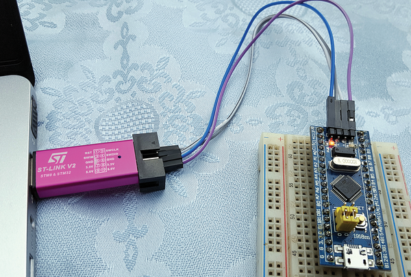 Figure 1: Connect the STM32F103C8T6 module to the programming adapter.
In order to configure a connection as an output switch for an LED, click with the left mouse button on the right in chip view, (for example on the PC8 connection). Next, select GPIO Output from the popup menu. CubeMX then highlights the connection as allocated in green and also marks it as set. If you want to reverse this operation, select the menu entry Reset state.
Now configure PA0 as GPIO Input and PA1 as ADC_IN1. In the list in the left column you'll see the resources ADC1 and SYS marked as allocated and carrying a yellow warning triangle. When you move the mouse over the ADC1 entry, a help notification appears explaining the reason for the warning: PA0 is no longer available for A/D conversion since it has been defined as a logic level input.
Now select the USART1 entry in the resource view and switch the mode from Disabled to Asynchronous. Then in the indicator, CubeMX marks the required connections (RX and TX) as allocated. If you move the mouse cursor over one of these connections, the popup menu will tell you that alternative allocations exist for these functions. If you also press [Ctrl] and click again on the connection, the alternative allocations will appear highlighted in blue. In order to change to an alternative allocation, press the mouse button and drag the functions to the new connection.
Listing 5
STM32F030F4P6.cfg
source [find interface/stlink-v2.cfg]
set WORKAREASIZE 0x1000
source [find target/stm32f0x_stlink.cfg]
reset_config none
In order to configure the serial interface, select the Configuration tab. Click on the USART1 button. Using the dialog that then appears, configure the baud rate as well as other parameters for the interface in the Parameter Settings tab. Now set up the support for interrupts (NVIC) and DMA in other tabs. Next confirm the dialog and select the ADC1 button. This button lets you activate the Continuous Conversion Mode.
Now switch to the Clock Configuration tab which indicates the clock rate distribution system. At first, the system governs all of the clock rates from the internal 8 MHz RC Oscillator (HSI). Next you will need to select HSE (High Speed External) as the clock rate since the VL Discovery and the STM32F103C8T6 module both have an 8 MHz crystal oscillator. This setting is grayed out though, so it can't be activated. Go back to the Pinout tab and select the RCC entry from the left hand column. In the roll down menu, you can now change the setting for HSE from Disabled to Crystal/Ceramic Resonator.
Switch back to the Clock Configuration tab. The system clock rate for the cortex CPU core FCLK can now be changed to 24 MHz. After this, the program will re-compute the corresponding settings. You can now convert the PLL source Mux to HSE. This causes CubeMX to mark the derived rates that cannot be used in red. Resolve these conflicts simply by clicking once on the Resolve Clock Issues in the tool bar.
Now save the project, preferably in a sub-directory in an Eclipse work area. This area can also be used later if you want to create a C project. Switch back to the Configuration tab and select the Generate source code based on user settings option from the tool bar. From here, select the SW4STM32 option as a Toolchain in the Project tab.
Look at the settings in the Code Generator tab. The setting at the very top is especially interesting. It is used to specify whether the required libraries end up as a reference or a copy in the project that is created. Pay attention to the options under HAL settings. The Enable full assert setting turns on large numbers of run time tests. When these are damaged, the program will lapse into an endless loop. The parameters for this loop will be the location of the damage exception.
After confirming the dialog now switch into a terminal window where you start converting the project that has been created into a makefile project (Listing 6).
Listing 6
Running CubeMX2Makefile.py
$ cd </path/to/converter>
$ ./CubeMX2Makefile.py </path/to/project>
Eclipse
You now need to import your project into Eclipse. To do this select the File | Import option from the menu in the development environment, open the C/C++ section in the dialog, and click on Existing Code as Makefile project. Click Next. From here, use the Browse button to search for the folder to find the makefile you generated earlier. Select the Cross ARM toolchain option below for the indexer (Figure 3). Finish the import with Finish.
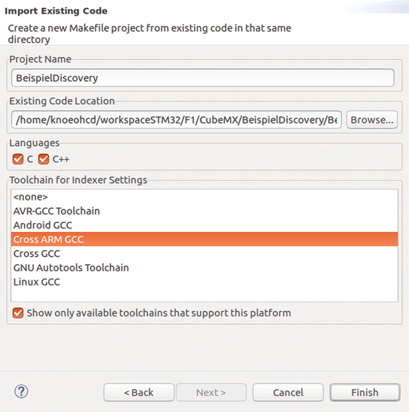 Figure 3: Using the import dialog in Eclipse to import your makefile.
At this point Eclipse will create a C/C++ project. The main.c is located in the sub-folder Src/. The main() function contained in this sub folder begins the process of initializing the controller with function calls and ends with an empty endless loop. Tutorials with the info required to carry out the initialization are available from Embedded Lab [7] or from Geoffrey Brown's e-book [8].
At first glance, you will see that there are numerous comments in the project. They divide the entire file into sections. Try to keep as many of these comments as possible for later modifications to CubeMX. Your changes should only be made in the areas marked with USER CODE. If you want to perform testing, you can use the program fragment from Listing 7. insert it in the main.c between the comments USER CODE BEGIN WHILE and USER CODE END 3 where it will replace the endless loop found there.
Listing 7
Test Fragment
.
.
.
/* USER CODE BEGIN 3 */
unsigned int delayInMilliSeconds;
while (1) {
  // Push the PA0 Button
  delayInMilliSeconds=HAL_GPIO_ReadPin(GPIOA, GPIO_PIN_0) ? 500 : 100;
  // Switch on PC8 (green LED)
  HAL_GPIO_TogglePin(GPIOC, GPIO_PIN_8);
  HAL_Delay(delayInMilliSeconds);
}
/* USER CODE END 3 */
.
.
.
During testing, we found that we still needed to correct the setting for make. To make the correction, use the right mouse button to call the project context menu in the Project Explorer and select the Properties entry. From there, switch to the C/C++ Build rubric and, in the dialog, remove the check mark from use default build command. Afterwards at the build command option, you can enter either the path to the make program (Windows) or just make.
Compile the program by clicking on the hammer icon or by calling Project | Build All. Check the project again in the Project Explorer. Next, select the option Run | Debug Configurations from the menu. In the dialog that appears, check GDB OpenOCD debugging in the list to the left. Now you can create a new configuration with a single click on the New icon.
To the right choose the Debugger tab and enter the parameters under Config options:. These parameters should be the same as those that you specified in OpenOCD during testing (Figure 4). make sure that the correct GDB call appears in the GDB client Setup under Executable:. Confirm the dialog with Debug.Eclipse will change to Debug view and wait on executing the program at HALInit().
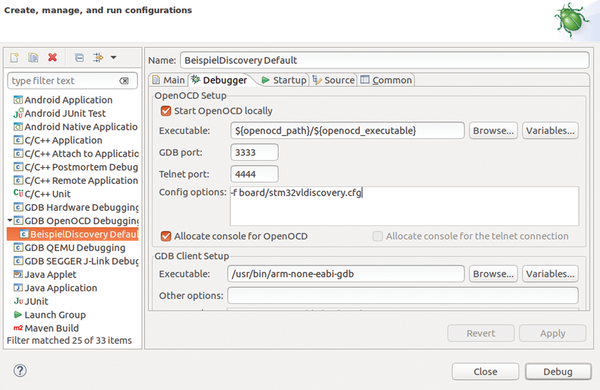 Figure 4: You can view information on program progress with the debugger.
The program can now be executed step by step. As soon soon as the execution reaches the conditional allocation of the variables delayInMilliSeconds, hold the mouse cursor for a few moments over the names of the variables. The context menu that opens gives you information about, among other things, the current value for the variables.
Next run the program using the green right arrow in the tool bar, and push the button on PA0. On the Discovery board this button will be blue. The frequency for the blinking should then decrease. The Hal library functions used in the program are explained in the API documentation for the HAL library [9].
« Previous 1 2 3 4 Next »
Buy this article as PDF
Pages: 7
(incl. VAT)
Buy Raspberry Pi Geek
US / Canada
UK / Australia
Related content
-
The CubeSat Project creates launch opportunities for schools

In the not too distant future the Raspberry Pi will take off from its humble beginnings on this planet and make a voyage into space. We review the CubeSat Project and talk to Patrick Stakem, an educator and pioneer of open source in space.
-
3D Slash CAD software works on a Raspberry Pi

Historically, Linux has not had many CAD offerings. Now 3D Slash has stepped in to fill the void, and it even works well on a Raspberry Pi.
-
The Switch Doc rebuilds his cat toy launcher with 3D printing

To explore the possibilities of 3D printing, we rebuild the cat toy launcher that debuted in Issue 5.
-
Raspberry Pi peer-to-peer communications

MQTT messaging controls multiple Pi music players from a smartphone.
-
Measuring and graphing resistance with a PicoBoard and a thermistor

We show how to use lists in Scratch to collect resistance measurements and graph the results with the pen tool.